


-
Academic Article
User Achievement | The Zhejiang University Team Uses Two-Photon Photoluminescence to Reveal How Dislocation Half-Loop Arrays Form in 4H-SiC Epitaxial Layers

Research Topic and Main Findings
The article presents a Journal of Physics D: Applied Physics study from the State Key Laboratory of Silicon and Advanced Semiconductor Materials and the College of Materials Science and Engineering at Zhejiang University. By combining photo-electrochemical etching with optical characterization, the team revealed the three-dimensional morphology of triangular defects and nearby dislocation half-loop arrays in 4H-SiC epitaxial layers, and confirmed tensile stress inside the triangular defects.
Figure 1: Research outcome
Key Finding: Internal stress within triangular defects is closely related to the nucleation, glide, and organization of basal-plane dislocations and half-loop arrays
Contribution of Two-Photon Photoluminescence
The article emphasizes that the two-photon photoluminescence capability of the UltraView MK-II multimodal nonlinear optical microscope provided non-destructive, high-resolution 3D imaging of 4H-SiC epitaxial layers. Using 752 nm near-infrared excitation, the researchers tracked the formation of dislocation half-loop arrays at different depths and confirmed that these defect arrays do not run through the entire epitaxial layer, but begin forming at about 5 um below the surface.
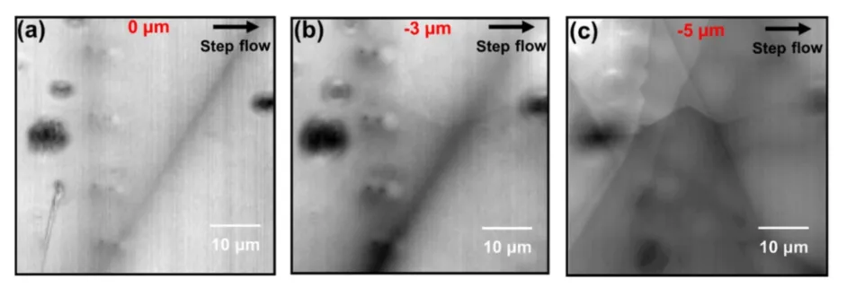
Figure 2: Three-dimensional imaging of dislocation half-loop arrays obtained with two- photon photoluminescence
Defect Visualization: The method distinguishes half-loop arrays from other defect-emission signals.
Practical Value: The findings support optimization of epitaxial growth, lower defect density, and improved device performance.
Significance of the Study
The study further argues that threading edge dislocations in the half-loop arrays are formed during epitaxial growth rather than inherited from the substrate. This has practical importance for reducing basal-plane dislocation density in thick epitaxial layers, lowering bipolar degradation risk in adjacent devices, and improving yield.
Popular Tags
-
Two-Photon
Recommendation
-
-
Academic Article
2026-02-09User Achievement | The Guizhou University Team Uses Stimulated Raman Imaging to Decipher the Efficiency-Boosting Mechanism of Enzyme Catalysis -
-
-
Academic Article
2026-01-22User Achievement | A New Breakthrough from the Peking University Team: Coherent Raman Reveals the Molecular Basis of Light-Regulated Hypocotyl Elongation -