



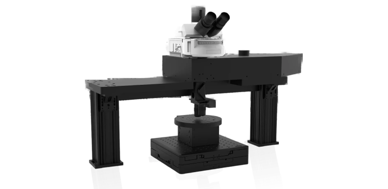
UltraView-2P-MK
UltraView-2P-MK I is based on two-photon nonlinear optical effects, using two photons to excite fluorescent molecules in the sample for high-resolution imaging. In wide-bandgap semiconductor wafer inspection, the system can efficiently identify micro-defects, impurities, and changes in material microstructure. Its inspection scope includes epitaxial-layer defect analysis, impurity distribution observation, and microstructural characterization. With high sensitivity and high resolution, UltraView- 2P-MK I meets the inspection needs of wide-bandgap semiconductors and provides reliable technical support for wafer production quality control.


Principle of Operation
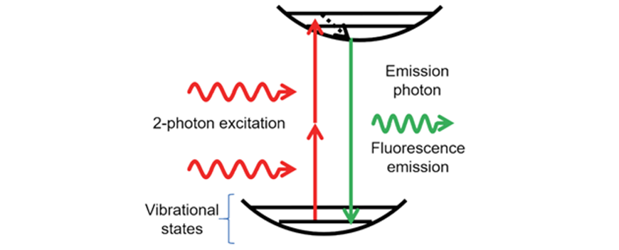
This advanced microscopy technique is based on nonlinear optics. Its core mechanism uses two-photon absorption under high photon-density conditions: fluorescent molecules simultaneously absorb two long-wavelength infrared photons, transition to an excited state, and then emit one shorter- wavelength photon. Imaging is achieved by detecting this emitted photon signal.
Core Advantages and Customer Value


-
 High-Resolution 3D Imaging Capability
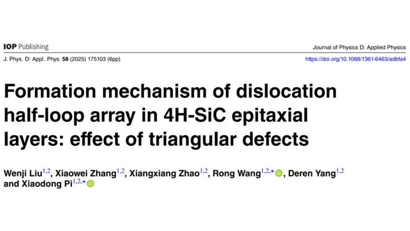
Lateral resolution reaches 0.4 um with a 60X water-immersion objective, while axial resolution is about 1 um. This enables clear identification of micron-scale and even nanoscale defects such as dislocations and impurities in silicon carbide. By combining 3D laser focal scanning with Z-axis stage movement, the system can achieve volumetric imaging beyond 30 um in depth and directly reveal internal defect trajectories, such as dislocation paths at the interface between silicon carbide epitaxial layers and substrates.

-
 Deep Penetration with Low Damage
Using near-infrared excitation wavelengths, the system is less affected by scattering in highly scattering samples such as silicon carbide epitaxial layers, delivering penetration depth far superior to visible-light single-photon imaging. A femtosecond pulsed laser with pulse width <=200 fs provides high peak power but low average power, with typical excitation power of 125-200 mW, minimizing sample damage and enabling repeat inspection of the same area.
-
 Flexible Imaging and Analysis
Broadband reflective scanning covers a spectral range of 0.4-20 um and can be paired with multiple laser wavelengths to match different sample emission characteristics. Beyond intensity imaging, the system can incorporate spectral analysis, such as distinguishing emission-peak differences between TSD and TED dislocations in silicon carbide, as well as transient-signal detection such as fluorescence lifetime, providing physical and chemical information about defects.
Applications
-

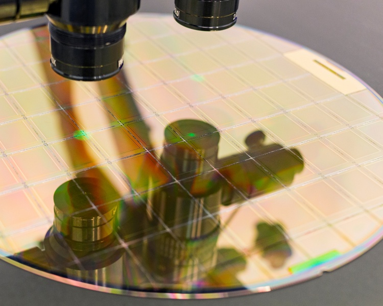 Silicon Carbide Defect Inspection
Detect different types of dislocation defects in silicon carbide and perform 3D imaging.
-
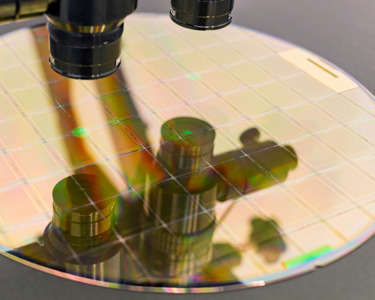 Gallium Nitride Defect Inspection
Perform 3D imaging for gallium nitride dislocation inspection.
-
Silicon Carbide Defect Inspection
Detect different types of dislocation defects in silicon carbide and perform 3D imaging.
-
Gallium Nitride Defect Inspection
Perform 3D imaging for gallium nitride dislocation inspection.
Technical Specifications

| Laser configuration | Microscope | Objectives | Electronic eyepiece | Photodetector |
|
center wavelengths 355nm / 515nm / 780nm / 1030nm average power 50-200 mW; repetition rate 80 MHz; pulse width ≤200 fs |
industrial upright gantry architecture, epi-illumination, optional fluorescence module | motorized switching among standard air objectives 4X / 20X / 40X, with optional upgrades | color CMOS camera, 30 fps, >=2K resolution | SI-PM/PMT |
| Stage |
Spatial resolution |
Imaging speed |
Field of view | Main functions |
Optional wafer vacuum chuck |
|
travel 200mm x 200mm x 20mm resolution 50μm repeat positioning accuracy ±0.5μm maximum speed 100mm/s |
≤400nm | 10FPS |
3000μmX3000μm with 4X objective 300μmX300μm with 40X objective |
wide-bandgap semiconductor wafer defect inspection large-area bright-field mosaic preview bright-field autofocus and auto-exposure large-area laser-scanning mosaic imaging 3D layer-by-layer laser-scanning imaging 2D / 3D rendering and image processing optional real-time laser focus lock |
8-inch wafer vacuum chuck compatible with 1- to 8-inch |

Downloads
-

Product Brochure
Wide-Bandgap Semiconductor Two-Photon Photoluminescence Inspection System - UltraView- 2P-MKProduct:UltraView-2P-MK